Advertisement


What really powers the cloud? Behind every Google search, A...
A lot of what defines a home isn’t visible at handover. I...
Private equity has played a significant role in shaping Indi...
Luxury real estate is one of the most talked-about segments ...
Airports play a much bigger role than just enabling travel -...
Samsung Electronics is reportedly considering setting up an advanced semiconductor packaging facility in Gwangju, South Korea, as demand for AI-related chips continues to grow. The proposed investment is expected to be discussed at an upcoming meeting between South Korea’s president and the heads of major business groups. The development comes as advanced chip packaging becomes increasingly important for AI applications, particularly high-bandwidth memory (HBM) chips. Separately, SK Hynix is also evaluating a new packaging facility in the country’s southwestern region, highlighting growing investment interest in semiconductor infrastructure linked to the expanding AI ecosystem.
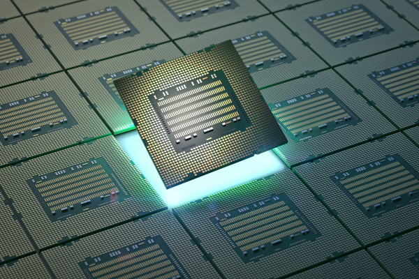
Samsung Electronics is evaluating plans to build an advanced semiconductor packaging plant in the southwestern South Korean city of Gwangju, according to a report by the Korea Economic Daily that cited industry sources.
The proposed investment is expected to be announced at a meeting scheduled for June 29 between South Korean President Lee Jae Myung and the leaders of the country’s largest conglomerates. The gathering, which will focus on a major shift in growth strategy, is expected to include Samsung Electronics Chairman Jay Y. Lee and SK Group Chairman Chey Tae-won.
The reported move comes as semiconductor companies increase investments in technologies supporting artificial intelligence applications. Advanced chip packaging has become a key segment of the semiconductor supply chain, helping improve performance by integrating multiple chips into a single package.
Separately, local newspaper Dong-a reported that SK Hynix is also considering the construction of a new chip packaging facility in South Korea’s southwestern region, particularly in South Jeolla Province. Both Samsung Electronics and SK Hynix declined to comment on the reports, while the presidential office stated that investment decisions are matters to be determined by individual companies.
If the project moves ahead, it would represent another step in Samsung’s efforts to strengthen its advanced packaging capabilities. The technology has become increasingly important due to growing demand for high-bandwidth memory (HBM) chips, which are widely used in AI servers and data centres.
Industry observers view the reported investment as a sign that Samsung may be preparing to accelerate spending ahead of a potential recovery and expansion cycle in the semiconductor industry, supported by rising AI adoption across sectors.
Demand for advanced packaging solutions has increased significantly in recent years as chipmakers seek higher performance and greater efficiency. HBM technology, which vertically stacks multiple DRAM chips, has emerged as a critical component for AI processors and computing systems.
Samsung supplies memory and semiconductor products to major technology companies including Nvidia, AMD and Google, all of which are investing heavily in AI infrastructure. The company has also been expanding its presence in the HBM segment as it competes more aggressively with market leader SK Hynix.
The latest report follows Samsung’s announcement in the past month that it had begun supplying samples of its newest 12-layer HBM4E memory chip to customers. The development was seen as an important milestone in the company’s efforts to strengthen its position in the fast-growing AI memory market.
Source Reuters
Advertisement


 Facebook
 Whatsapp